# ASE expands PowerSiP for power delivery beneath AI processors
> ASE says its PowerSiP expansion lets designers place voltage-regulator modules beneath AI processors. Its claimed 50% or greater reduction concerns parasitic routing losses; the public pages give no test method or system-level measurement.
By BIG CHANGE Editorial
Published: 2026-10-14T23:35:17.574Z
Updated: 2026-10-14T23:35:17.574Z
Canonical: https://bigchange.ai/blog/ase-powersip-vertical-ai-processor-power-delivery
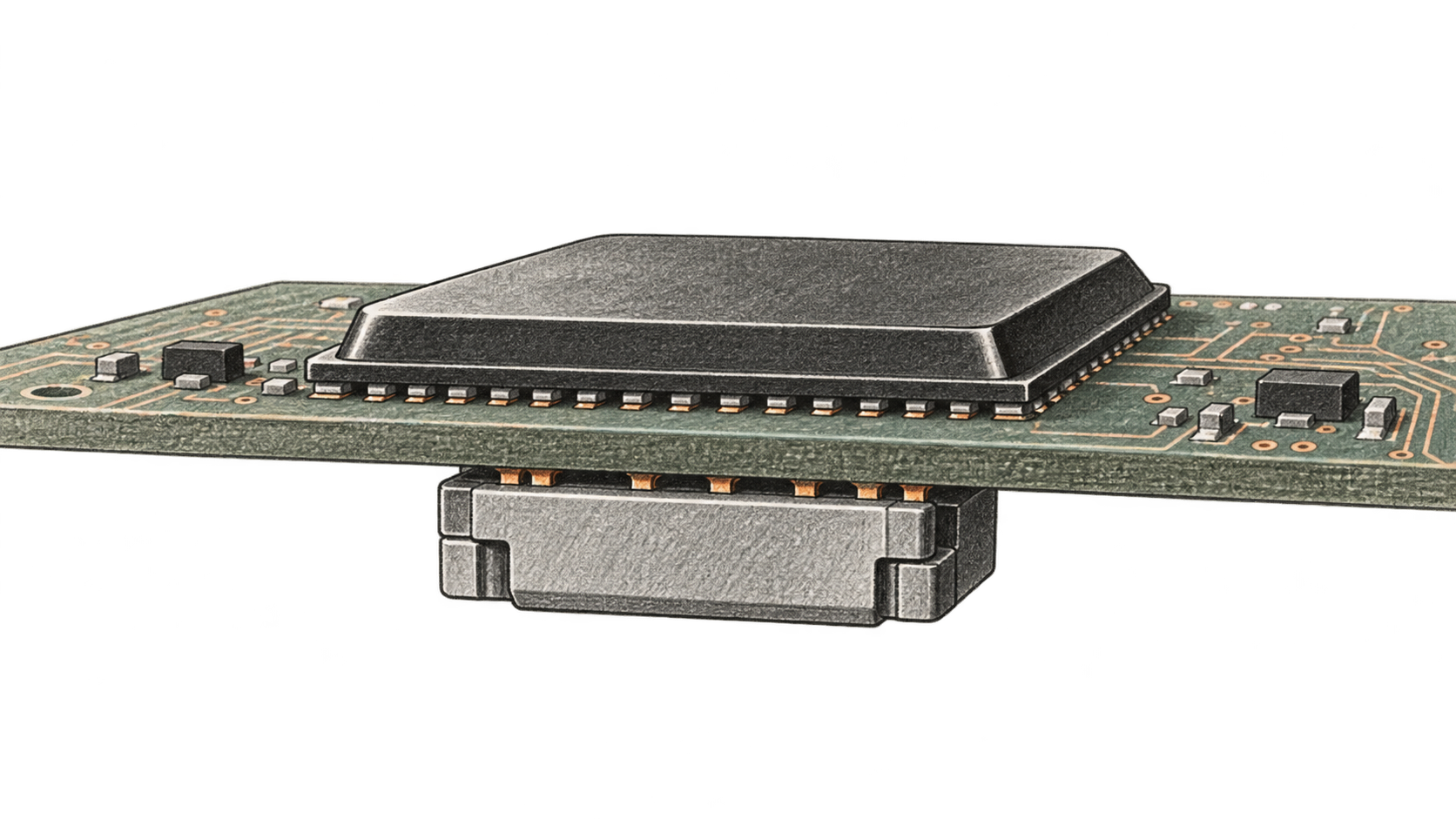
AI-generated conceptual illustration by BIG CHANGE; generic hardware relationship, not an ASE product rendering, engineering drawing or measured result.
**Dek:** ASE says its expanded PowerSiP platform lets designers place voltage-regulator modules beneath AI processors. Its claimed 50% or greater reduction concerns parasitic routing losses, with no public test method or system-level measurement.
ASE announced an expansion of its PowerSiP platform on October 13, 2026. The company describes a 3D system-in-package assembly toolbox for voltage-regulator modules (VRMs) that can sit directly beneath an AI processor. It says the solution is available now. The design moves the final voltage-regulation stage from a lateral board layout to a shorter vertical route into the chip.
## The big change
- **What changed:** ASE has expanded the packaging options for putting the final voltage-regulation stage beneath an AI processor. That arrangement shortens the board-to-chip route described in its public materials; it does not specify a complete VRM design for every processor.
- **Why it matters:** AI-server designers must deliver high current through limited space around a processor. A shorter route gives power and package engineers another architecture to assess where routing loss and tray thickness constrain the design. ASE's claimed loss reduction concerns that route, while the effect on a complete server remains unmeasured in the public material.
- **What to watch:** A buyer's decision turns on a disclosed test comparison, electrical and mechanical specifications, integration requirements and price. ASE's public release and product page do not supply those details, and its technical brief requires a contact form.
## The current path ASE wants to shorten
In the lateral arrangement described in [ASE's announcement](https://ase.aseglobal.com/press-room/ase-expands-powersip-platform-for-next-generation-ai-power-delivery/), current leaves the voltage regulator, travels across the printed circuit board, then passes through package substrates and interconnects to reach the processor. ASE says high-performance AI systems-on-chip can draw peak currents above 1,000 amps at less than one volt. At that scale, it argues, losses along the route become consequential.
PowerSiP's vertical arrangement puts the voltage-regulation module on the back side of the board, directly below the processor. The high-current route from regulation to chip is shorter. ASE presents this as a way to fit thin, dense VRMs into compute trays while reducing losses associated with the routing path. Its [PowerSiP product page](https://ase.aseglobal.com/powersip/) describes the same below-processor placement and board-to-chip direction. Neither public source supplies a board drawing with dimensions or a processor-specific integration recipe.
The announcement lists building blocks rather than a named finished VRM. One option sandwiches double-sided connected capacitors between coreless substrates. Another uses substrate-less, solder-free capacitor-array modules with exposed terminals for embedded-substrate or PCB integration. ASE also lists 4:1 high-aspect-ratio copper pins, which it says lower package impedance, plus dense active and passive component integration using single- or double-sided molding. These are the company's described assembly options; the public material does not say which combination forms a particular customer module.
## What the 50% figure measures
ASE says shortening the high-current transmission path can reduce **parasitic routing losses by 50% or more**. Those are losses associated with the electrical route between the regulator and processor. The phrase does not give a processor, server or data-center energy measurement. The release and product page provide no public test protocol, comparison design, operating conditions or denominator detail sufficient to recalculate the claim. BIG CHANGE has not tested the hardware or independently verified the result.
ASE links the routing-loss claim to better system efficiency, but its public materials do not quantify the resulting change in VRM efficiency, processor power, server energy or facility electricity use. Buyers would need measurements for their own power-delivery design before assigning a system-level benefit to the architecture.
## What a buyer can assess today
The two public ASE pages establish the intended location of the regulator, the named packaging options and the scope of the vendor's loss claim. They do not identify a specific SKU or product version, customer deployment, processor compatibility, electrical ratings for a finished module, price or qualification results for a named system. “Available now” is ASE's statement about its solution; the announcement does not establish that a specified module can be ordered for a particular accelerator.
ASE offers a PowerSiP technical brief through a form requesting name, company and email. Without that document or direct engineering specifications, a power or package team cannot reproduce the 50% comparison from the public pages. The useful next step in an architecture review is to request the test conditions and module-level specifications, then compare a candidate vertical design with the team's own lateral layout under the same load and thermal constraints.
[BIG CHANGE's report on planned GlobalFoundries and TSMC silicon-interposer supply](https://bigchange.ai/blog/globalfoundries-tsmc-us-silicon-interposer-ai-packaging) covers another part of AI chip packaging: manufacturing capacity for an interposer, rather than this power-delivery path.
## Sources & further reading
- [ASE: PowerSiP expansion announcement](https://ase.aseglobal.com/press-room/ase-expands-powersip-platform-for-next-generation-ai-power-delivery/) — October 13, 2026. Primary source for the availability statement, lateral and vertical path descriptions, component toolbox and attributed claim about parasitic routing losses. It does not publish the test method or a measured system-level energy result.
- [ASE: PowerSiP product page](https://ase.aseglobal.com/powersip/) — current page, checked October 15, 2026. Describes below-processor placement and package options. Its technical brief is offered through a form requesting name, company and email; the public page does not provide pricing or a finished-module specification.
## Sources
- [ASE Expands PowerSiP Platform for Next-Generation AI Power Delivery](https://ase.aseglobal.com/press-room/ase-expands-powersip-platform-for-next-generation-ai-power-delivery/) — Dated official announcement; attributes the 50%+ reduction to parasitic routing losses and says the solution is available now. No public methodology, whole-system measurement, pricing or customer deployment.
- [powerSiP](https://ase.aseglobal.com/powersip/) — Current official platform page describes vertical board-to-chip power delivery, system-in-package components and toolbox. Technical brief requires contact information; page has no version, pricing or public benchmark method.
The BIG CHANGE newsletter
The big picture. At your pace.
Recent stories on AI and robotics, the shifts worth watching and practical ideas to use. Choose a daily briefing, weekly digest or monthly perspective.
Next scheduled send (UTC): . Your first edition arrives at the next scheduled send after you confirm.
Your privacy, your choice.
Necessary storage supports site security and remembers your choices. Optional Google Analytics stays off until you allow it. You can read every story with necessary storage only. Privacy details