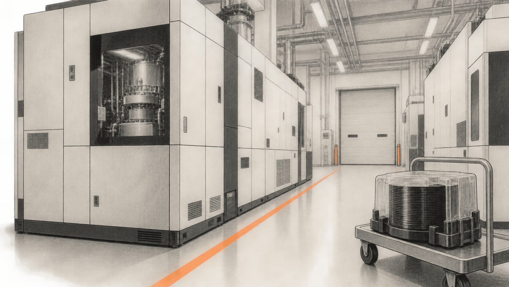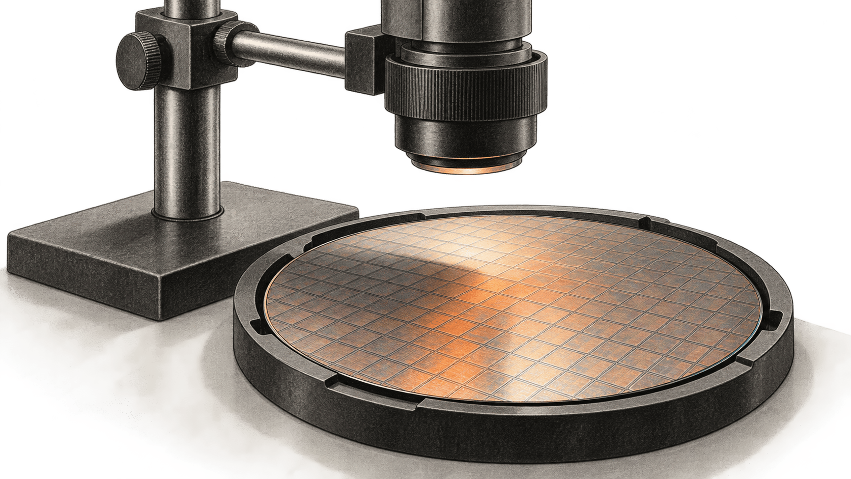
NVIDIA's October 14 SEMICON West announcement spans several different kinds of semiconductor work: modeling materials, designing and verifying chips, simulating manufacturing, and inspecting production output. The release calls this an advance toward “AI-defined fabs.” For an engineering team, the immediate choice is narrower. Some underlying libraries have public documentation and downloads; the new atomic-simulation library is in early access, and several named partner integrations are plans or vendor-reported results.
The big change
- What changed: NVIDIA introduced cuPotential for atomic-scale simulation in early access and described partner uses of existing GPU libraries, AI models and agents across design and fab workflows.
- Why it matters: The announcement connects tools at different stages of the chipmaking chain. A team can inspect some library interfaces today, while access to a partner's integrated product depends on that partner's release and commercial terms.
- What to watch: NVIDIA's additional 2–3x cuPotential result comes from early-access tests on workflows already optimized for GPUs. The release does not give a public test setup, broad availability date or price. BIG CHANGE did not test the library.
A simulation library is not an AI agent
NVIDIA describes cuPotential as GPU-accelerated functions that developers can add to software for modeling electrical forces and other interactions among large numbers of atoms. An agent could call that modeling software, inspect results and choose another run. The library performs the numerical work; the agent organizes the sequence. NVIDIA names Synopsys as an early adopter, but the release only offers early access to cuPotential and does not publish a general download, integration instructions, hardware requirements or price for it. Its 2–3x figure is NVIDIA's early-access result against already GPU-optimized workflows, not an independently reproduced gain or a comparison with CPU-only software.
The same distinction applies higher in the design flow. NVIDIA says Synopsys is using cuPotential, cuEST and cuDSS in simulations, while its AgentEngineer tools interoperate with Nemotron models and NeMo for design and verification agents. Those are separate layers: models and agent tooling guide work; numerical libraries accelerate specified calculations; Synopsys' EDA applications supply the engineering workflow. NVIDIA also reports early QuantumATK and S-Device speed results, but the release does not provide public benchmark inputs or configurations that would let a buyer transfer them to a different job.
For a library an engineer can inspect directly, cuDSS documentation describes a preview GPU solver for sparse linear systems, with downloads and examples. Its API may change. An engineering software developer can evaluate that solver with a representative matrix and check numerical and runtime behavior in their own environment. This is a different access path from adopting a named partner's commercial EDA or multiphysics product. NVIDIA says Cadence uses cuDSS with Celsius in an AuraStack packaging example; the claimed 8x heat-and-stress optimization is a vendor result, with no reusable workload or purchasing terms in the announcement.
Manufacturing and inspection have separate release paths
For mask preparation, Siemens' October 14 release says it integrated NVIDIA cuLitho with Calibre manufacturing software for optical proximity correction. Siemens reports up to 12x acceleration on full-chip workloads. The release describes an integrated commercial workflow, not a free-standing Calibre feature that every customer can turn on without checking product configuration, GPU infrastructure and licensing. It gives no public price or reproducible workload for that figure.
For three-dimensional process modeling, NVIDIA says Lam Research intends to integrate the open-source NanoVDB data structure into SEMulator3D, targeting release by the end of 2026. OpenVDB's NanoVDB documentation is public, so developers can examine that component now. It is not proof that Lam's integration is already shipping. NVIDIA attributes an expected up-to-30x result to selected wafer-etch modeling, rather than to every SEMulator3D task. The SEMulator3D product page describes Lam's existing virtual process-modeling product; access to a future NanoVDB-enabled version remains a separate question for Lam.
Inspection has a more immediate library route. NVIDIA Performance Primitives is available through the CUDA Toolkit and documents GPU image-processing operations. NVIDIA says KLA used production-kernel insights in an NPP normalized cross-correlation kernel and measured it against older CPU versions. That account establishes what KLA and NVIDIA report, not general inspection-system throughput or a newly available KLA product. A developer can inspect NPP's documented image operations today; adopting KLA's equipment workflow requires its own product and deployment information.
Fab and test operations form another category. NVIDIA says Advantest has integrated Nemotron and an anomaly model into its ACS real-time data infrastructure to recommend corrective actions for test cells. Advantest's product page describes monitoring live tester data and presenting anomaly and diagnostic insights to engineers. That is a vendor-described operational application, not a simulation library that a developer downloads or proof that corrective actions are autonomous. The public page does not give deployment prerequisites, prices or measured outcomes for a specific customer.
These paths suggest different next steps. Teams building simulation code can examine public cuDSS, NanoVDB and NPP materials and benchmark a representative task. Teams evaluating cuPotential need early-access terms and implementation details from NVIDIA. Buyers of Calibre, SEMulator3D, Advantest ACS or other partner systems need a product-specific release, supported configuration, license and workload-level evidence. The October 14 release does not settle the total cost of those combinations or demonstrate a complete autonomous fab.