# Nvidia financing SPIL chip-packaging expansion, Reuters reports
> An unnamed executive described billions for capacity; Nvidia did not respond to Reuters.
By BIGCHANGE.AI Editorial
Published: 2026-11-07T18:12:38.115Z
Updated: 2026-11-07T18:12:38.115Z
Canonical: https://bigchange.ai/blog/nvidia-spil-cowos-packaging-financing-report
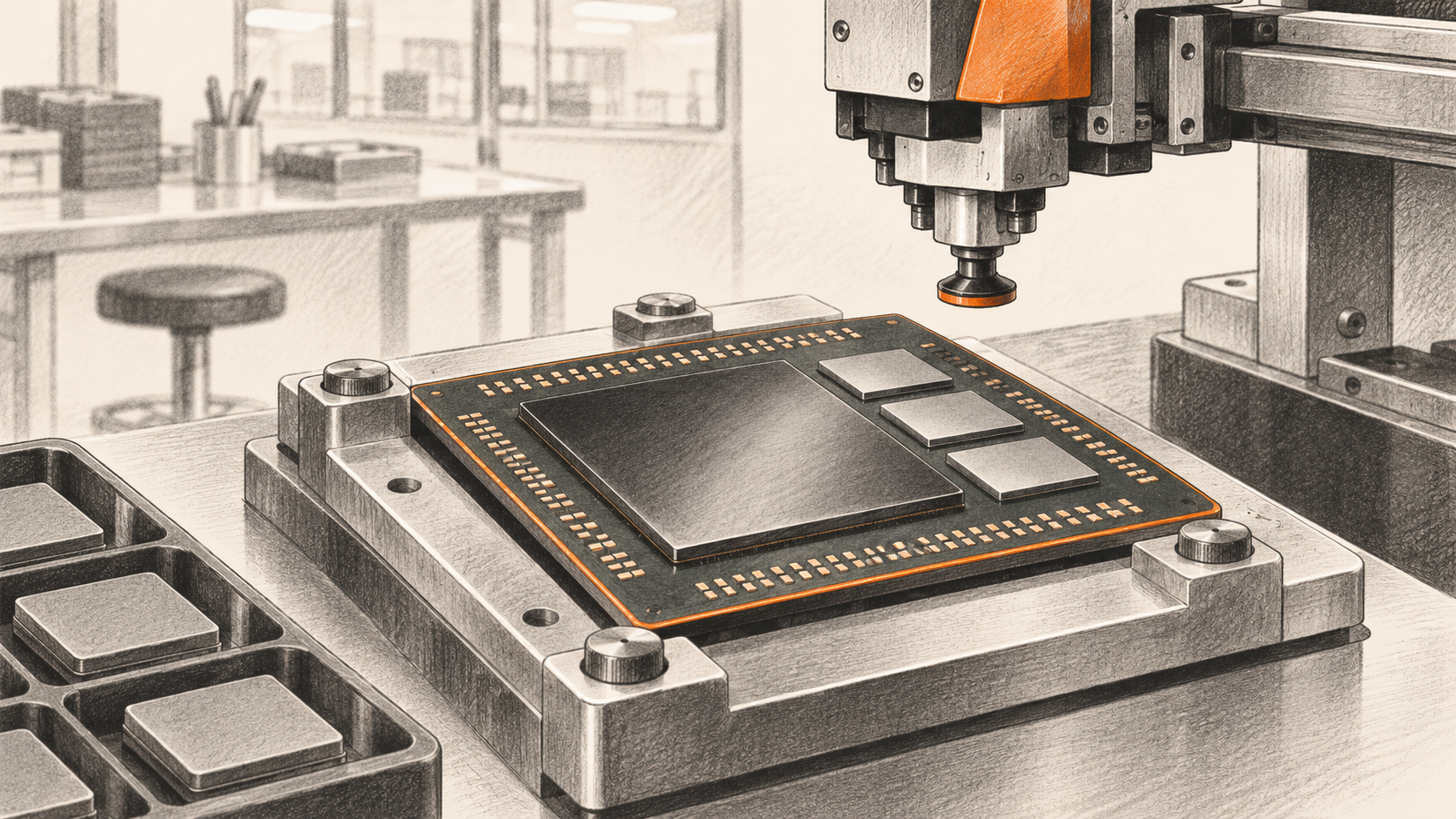
AI-generated conceptual illustration; not an actual SPIL facility or production process.
Nvidia is providing billions of dollars to help expand advanced chip-packaging capacity at Siliconware Precision Industries, according to a [November 6 Reuters report](https://www.investing.com/news/stock-market-news/ai-boom-turns-chip-packaging-into-the-next-battleground-for-semiconductors-5006549) citing one unnamed industry executive. The reported financing would support new factory space and equipment at SPIL, a unit of Taiwan’s ASE Technology.
Nvidia did not respond to Reuters’ request for comment. ASE said it does not comment on market rumors involving customers.
## The big change
- Reuters reports funding for additional CoWoS packaging capacity, an important stage in assembling powerful AI processors.
- Packaging joins separate components into a system; making more individual chips does not by itself complete that work.
- Nvidia and ASE have not confirmed it.
## Why packaging matters
A processor and its memory begin as separate pieces of silicon. Advanced packaging brings them together so they can exchange data through dense connections. [TSMC describes](https://www.tsmc.com/english/dedicatedFoundry/technology/cowos) its CoWoS family as integrating system-on-chip dies and high-bandwidth memory stacks; different CoWoS variants use different interposer approaches.
An interposer provides a connection layer between components, rather than being the finished processor itself. Bringing memory near the processing die enables a wide connection between them, which is useful when AI workloads need to move large amounts of data. Packaging capacity is therefore a distinct part of the supply chain from making the logic chips or the memory.
The report leaves financing terms, site, schedule and additional capacity unspecified.
## Separate projects, separate claims
On October 21, [Nvidia announced](https://nvidianews.nvidia.com/news/nvidia-and-supply-chain-partners-expand-capacity-to-accelerate-ai-infrastructure-buildout/) a separate plan with SPIL to expand optical-engine manufacturing in Taiwan for co-packaged optics. It targeted a 15-fold increase by mid-2027 and aimed to double capacity again by the end of 2028. Those are targets for optical components, not confirmation of the CoWoS financing reported by Reuters.
Another part of the chain is the interposer itself. In October, [GlobalFoundries announced](https://gf.gcs-web.com/news-releases/news-release-details/globalfoundries-reaches-agreement-establish-us-based-supply) a $2 billion manufacturing agreement to supply silicon interposers for TSMC’s CoWoS ecosystem from New York, with a production ramp expected in the first half of 2028. BIG CHANGE [covered that agreement](https://bigchange.ai/blog/globalfoundries-tsmc-us-silicon-interposer-ai-packaging); it is distinct from the reported SPIL financing.
Optical engines and silicon interposers serve distinct functions in AI infrastructure. Actual impact depends on when added capacity and other components become available.
## Sources
- [Reuters: chip-packaging investment](https://www.investing.com/news/stock-market-news/ai-boom-turns-chip-packaging-into-the-next-battleground-for-semiconductors-5006549) — November 6 report; unnamed source and company responses.
- [TSMC CoWoS technology](https://www.tsmc.com/english/dedicatedFoundry/technology/cowos) — Manufacturer explanation of packaging variants.
- [Nvidia supply-chain plans](https://nvidianews.nvidia.com/news/nvidia-and-supply-chain-partners-expand-capacity-to-accelerate-ai-infrastructure-buildout/) — October 21 optical-engine targets; separate project.
- [GlobalFoundries and TSMC agreement](https://gf.gcs-web.com/news-releases/news-release-details/globalfoundries-reaches-agreement-establish-us-based-supply) — October announcement of interposer supply plans.
The BIG CHANGE newsletter
The big picture. At your pace.
Recent stories on AI and robotics, the shifts worth watching and practical ideas to use. Choose a daily briefing, weekly digest or monthly perspective.
Next scheduled send (UTC): . Your first edition arrives at the next scheduled send after you confirm.
Your privacy, your choice.
Necessary storage supports site security and remembers your choices. Optional Google Analytics stays off until you allow it. You can read every story with necessary storage only. Privacy details