NVIDIA's October 21 agreements and expansion plans with six suppliers put dates on a less visible part of the AI infrastructure buildout: the work needed to turn fabricated chips into usable packages, test them and connect them in large systems. Some supply is available now. Much of the additional capacity NVIDIA describes is scheduled for 2027 or 2028.
The company said it aims to raise substrate capacity for its products to 2.5 times the current level over three years. It expects total semiconductor testing capacity to double from 2026 to 2027. Those are company targets for different manufacturing steps, with no absolute production baselines in the announcement; they cannot be added into a single forecast of finished systems.
The substrates and interposers have different jobs
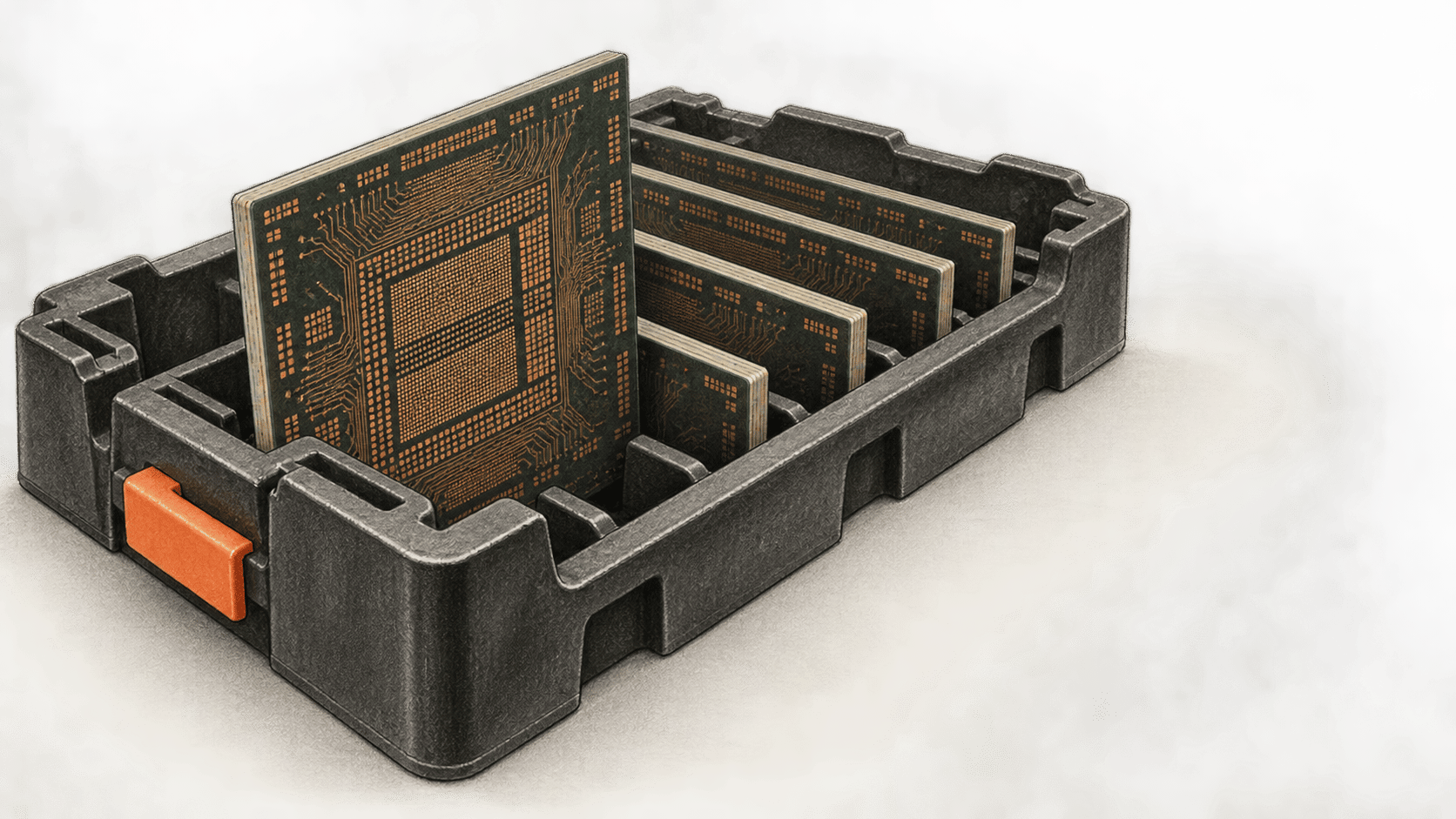
A package substrate carries connections from the chip package to the circuit board. An interposer provides denser connections among components inside a package, such as logic chips and memory. IBIDEN's description of package substrates and SemiEngineering's advanced packaging guide show why extra capacity at one layer does not replace capacity at the other.
NVIDIA says Samsung Electro-Mechanics is joining its substrate supply chain with capacity from existing South Korean operations. Planned facility upgrades and new factories would add to that. Unimicron's expansion in Taiwan is expected to start adding substrate capacity in the second quarter of 2027 and reach full capacity by mid-2028. At IBIDEN's Ono plant in Japan, NVIDIA says a previously announced multibillion-dollar capacity reservation advance supports a target of three times the plant's current capacity, with additional capacity beginning to ramp in the first quarter of 2028. IBIDEN disclosed a wider investment plan in February and reported that Ono's initial operations began in 2025. The plant's existing operation and its proposed further ramp are separate facts.
For interposers, NVIDIA and Amkor target a greater than 300% increase in interposer wafer capacity in South Korea by the end of 2028. That is an increase of more than three times the starting amount, rather than a final capacity of 300% of it. Amkor announced a separate $1.3 billion agreement supporting its South Korea expansion on October 21. It said its multiyear NVIDIA agreements in Arizona and South Korea total $3 billion. Neither company's announcement gives a present interposer wafer count or a dated volume of completed NVIDIA packages from the new lines.
Testing and optical engines carry their own schedules
After packaging, chips still require testing. NVIDIA says a $1.1 billion capacity reservation advance to King Yuan Electronics (KYEC) will support new US facilities and equipment, with high-volume production targeted for April 2027. Expanded Singapore testing operations are expected to reach high-volume production in February 2027. The announced doubling of total testing capacity refers to NVIDIA's 2026-to-2027 plan, not just the KYEC site.
Siliconware Precision Industries (SPIL) addresses a different part of the system: optical engines for co-packaged optics. These place optical communications components alongside a network switch chip, as NVIDIA's technical explanation describes. NVIDIA says SPIL targets 15 times its optical-engine capacity by mid-2027 and aims to double that again by the end of 2028. This is a plan for networking components, not a count of additional GPUs.
The big change
NVIDIA has attached named suppliers, advance financing and staggered dates to four distinct production steps. Existing Samsung substrate capacity is the near-term addition described in the release; most specified new ramps fall in 2027 and 2028. Supplier investment and a reserved share of future capacity can help prepare production, but the announced ratios do not establish how many completed AI systems will ship or when. The useful milestones now are whether each facility reaches its stated ramp and whether substrate, interposer, testing and optical-engine output advance together.
Sources & further reading
- NVIDIA's October 21 supply-chain announcement sets out the six suppliers, capacity targets and proposed dates. Its quantities are forward-looking company statements without absolute output baselines.
- Amkor's October 21 agreement disclosure supplies the $1.3 billion South Korea agreement and $3 billion combined agreements figure. It does not report completed new South Korea output.
- IBIDEN's investment notice and Ono plant account establish the earlier investment plan and existing plant operations; NVIDIA supplies the latest threefold Ono target and ramp date.
- SemiEngineering's advanced packaging guide explains the different connection layers within a semiconductor package. NVIDIA's photonics explainer identifies the optical-engine role in its switches.